Carbon
nanostructures
Investigators:
V. Osipov, D.
Kolesnikov, V. Katkov
Introduction
Carbon nanocones
Fullerenes
Carbon nanotubes
Negatively curved nanostructures
Electronic structure of various nanoparticles
Conclusion
References
Introduction

At
the present time, carbon nanostructures are regarded as artificially
composed structures with the nanometer size. Their properties are
the subject of both theoretical and experimental investigation; nowadays
they have a very wide range of possible applications (see, for example,
[1]).
The
history of carbon nanostructures begins in 1985, when the Buckminsterfullerene
C60 was discovered by Croto[2]. Since
that time, the number of discovered structures is rapidly increasing.
The examples of them are: the nanotubes discovered by Ijima [3],
the family of fullerenes C70, C76 [4],
C84 [5], C60 in a crystalline form,
carbon nanocones [6], carbon nanohorns
[3], nanoscale carbon toroidal structures
[7] and helicoidal tubes [8],
periodical carbon structures Schwarzites (proposed in [9])
and Haeckelites [10], etc. These carbon
structures could be singlewalled or multiwalled; they may have zero,
positive or even negative Gaussian curvature (Schwarzites). Recently,
a few types of similar non-carbon structures were discovered: for
example, boron nitride nanotubes [11],
molybdenum disulfide or tungsten disulfide structures [12]
and even the silicon nanotubes [13]!
In this review, the topics of doped carbon nanostructures and combined
nanostructures (fullerenes in the nanotube or the peapod structures,
metal inside fullerenes etc.) will not be discussed in detail, due
to the boundlessness of this subject.
|
|
As it was well known before 1985,
carbon could form two types of lattice: the diamond lattice
with sp3 - hybridization, where each atom is connected with
four others, and the graphite lattice. Graphite is formed by
flat hexagonal layers of carbon atoms, separated by 3.35 Å (angstroms),
and the distance between each two nearest carbon atoms in the
layer is 1.42 Å. The bonding energy of two atoms located in
the same layer exceeds the same energy for different layers,
and as a good approximation one can consider these atoms as
having sp2 - hybridization.
|
|
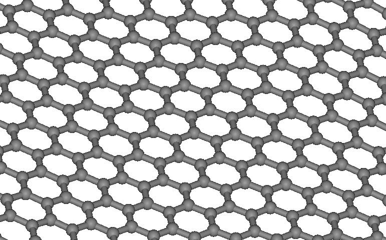
Figure
1. The bended graphene layer
|
It is interesting to note that the bonding energy for
the graphite between atoms in the same layer is as strong as the bonding
in the diamond structure, although the solidity of graphite, determined
by interlayer bonding, is very low. All the carbon nanostructures
known at the present time could be constructed from an ordinary hexagonal
graphene layer. Another key concept of the carbon nanostructures is
disclination, which is presented in the lattice as five- or sevenfold,
or (scientifically speaking) topological defect of rotation. Let us
imagine a plane with hexagonal network on it, where each atom is connected
with three others (see Fig.1). The length of each connection has a
tendency to remain unchanged, and if we bend the plane, it will straighten
up. The simplest way to change the planes shape is to cut the sector
from the plane and glue its opposite sides.
|
|
According to the fact, that our
plane is made of the hexagons, we can cut the sector with the
angle multiple of 2p /6. When the
cut is made, there will appear five-, four- or even threefold.
The lattice, trying to minimize its potential energy, will bend
into a conical surface. Finally we got the most simple carbon
nanostructure - the carbon nanocone (see Fig. 3). On the other
hand, we can insert the sector of the lattice between the cuts,
which gives the sevenfold, or octagon, etc. In the first case,
the Gaussian curvature of the surface (a well-known local geometrical
parameter) will be positive. In the second case, it will be
negative.
|
|
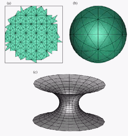
Figure
2. The plain (a), the positively (b) and the negatively (c)
curved surfaces
|
The most common example of the surface with positive
Gaussian curvature is the sphere shown on the Fig. 2 (b), while the
onesheet hyperboloid (Fig. 2 (c)) has negative curvature. The plain
and the cylinder is, according to the differential geometry, non-curved
surface with exact zero Gaussian curvature. So, the presence of the
pentagons in the hexagonal network leads to the positive curvature,
and the inclusion of the hexagons leads to the negative sign of the
curvature. It will be shown that carbon nanostructures could have
all the geometries listed above.
Carbon
nanocones
|
|
Carbon nanocones, discovered in
1994 [6], are the most simple
example of the nanostructured carbon. They are made, as a rule,
of the hexagonal plane with a different number of pentagonal
defects, more precisely, from one to five. Each cut, or the
pentagonal disclination, has the angle 2 π /6. As it was
shown in [14], the fivefold (or
positive disclination) could be stable, but the most stable
configuration for more than one defect is the configuration,
where they are separated by hexagons (the isolated pentagon
rule) [15].
The nanocones are produced by
carbon condensation on a graphite substrate [6],
and by pyrolysis of heavy oil [16].
Another method of their formation is laser ablation of graphite
targets [17].
|
|
Figure
3. The carbon nanocone
|
|
|
Theessence of the method is heating
the graphite surface with intensive short laser pulse, which
evaporates some number of atoms from the graphene sheet, and
other atoms rearrange into the conical surface described above.
So, the laser beam here plays the same role as the cut and glue
procedure. One needs to notice that the mechanism of nanostructure
growth has not been studied enough yet.
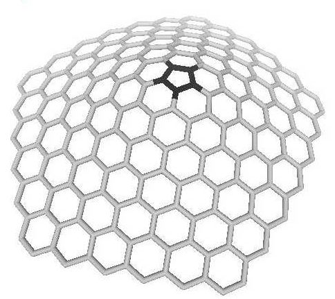
There is also one special class
of nanocones, called nanohorns (they look like animals horns)
with exact five defects (fivefolds) on the tip [3],
Fig.4. They could be produced by the method similar to the nanocones,
by use of laser ablation, even on the open-air [18].
These structures with good electron emission properties are
easy to get and stable enough [19].
Both nanohorns and nanocones are believed to have good field
emission properties, which determine their usage as electron
field emitters.
|
|
Figure
4. The carbon nanohorn
|
As for the theoretical prediction of electronic properties
of the nanocones, this is still a discussionable topic (see Chapter
6). One may say, that various models predict the increase of the electronic
density of states for the cones. For some classes of the cones, there
could be a metallic behavior; for example, the nanohorns could be
metallic (even if they have a very big length) due to the calculations
described in the Chapter 6. The metallization is in good agreement
with the experimental measurements of the emission properties [19].
However, this subject is still left open.
Fullerenes
|
|
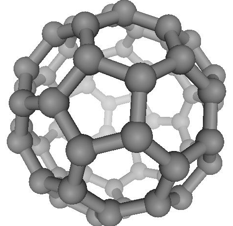
The
history of fullerenes begins in 1985, when Kroto with colleagues
carried out an experiment to simulate the condition of red giant
star formation, when cold carbon clusters are produced. With the
use of the mass-spectrometer, they found a large peak commensurate
with 60 carbon atoms. After intensive discussions, they concluded
that this construction could be a truncated icosahedron, or the
Buckminsterfullerene C60 (see Fig. 5). Since that time, the family
of fullerenes (closed spherical carbon structures) increased,
and now it consists of C70, C76, C84, C240, C540 and so on. A
careful reader, when looking at Fig. 5, could find the same hexagons
and fivefolds, as in the nanocones. |
Figure
5. The Buckminsterfullerene |
Indeed, one can produce the fullerene from the graphene
layer with the same imaginary cut-and-glue procedure but with one
important difference: the number of cuts (fivefolds) should be exactly
twelve. Actually, in view of the fact that the fullerene is a closed
structure, one could notice, that to produce the bounded piece of
lattice, we need to cut the sector with the full angle 2p
. Thus the fullerene could be made of two such pieces (the upper and
the lower one), and the full cutting angle for the fullerene is 4p
, or twelve times by 2p /6. More precisely,
we need to take into account the genus of the structure: as it is
shown in [15], it determines the number
of squares, fivefolds, sevenfolds and octagons in the lattice. For
the closed structure with genus zero, when the lattice is composed
of pentagons and hexagons, the number of pentagons should be exactly
twelve.
The fullerenes, being closed structures with zero genus,
differ by their shape and symmetry. The Buckminsterfullerene C60,
shown in Fig. 5, has a spherical-like shape and the full group of
symmetry of the icosahedron Ih. This fact means that it could be rotated
by the angle of 2p /5 around the center
of each pentagon and reflected in the mirror located on the each plane
of its symmetry. Another class of spherical fullerenes like C140 and
C260 (proposed in [15]) lacks the mirror
symmetry h, and their maximum symmetry group is icosahedral (I). There
is also a class of non-spherical fullerenes, the most famous of them
C70 the Rugby Ball, with an ellipsoidal shape. One should also
note that all of the fullerenes have the same Gaussian curvature sign
(positive) , therefore all of them have a convex surface.
Due to the small size, some individual properties of
fullerenes are now under investigation, but as it was shown in [20],
the fullerenes could appear also in the crystalline form. According
to the authors cited above, the doped structure of C60 crystals is
superconductive at 33 K (but this fact is not proved yet well enough).
When one is speaking about the fullerenes, one should
mention an interesting property of these closed structures the ability
for holding the molecules inside (hence the fullerenes are potential
nano - capsules). The nano capsule is a closed nanostructure (the
fullerene or the nanotube) with one or more atoms of the substance
inside the structure. Experimentally there were detected the nano
- capsules like a metal inside - fullerenes La@C60, La@C70, La@C74,
La@C82, capsulated radioactive materials U@C28, Gd@C82, the peapod
structures (fullerenes inside the nanotube) C60@SWNT, and so on. For
the substance enclosed in the fullerene nano-capsule, carbon atoms
act like a defense shield: the experiments show that the fullerene
containers are good for protecting their contents from water and acid.
Some interesting magnetic properties of the ferromagnetic metals (Fe,
Co, Ni) inside the fullerenes were observed; namely, the magnetic
properties of the metals remain unchanged. As for the capped radionuclides,
the stability of these metallic fullerenes could bring the new effective
solution of the radioactive waste elimination. There is also an interesting
substance called Technegas (it is used in the medicine), discovered
in 1984. The production method of this gas appears to be very similar
to the production method of the fullerenes; actually, it appears to
be big (from ten to one hundred nanometers) carbon nanocrystals with
the metastable technetium atoms inside. Consequently, this substance
was the first commercial application of the filled carbon structures
before the discovery of the fullerene in 1985.
Carbon
nanotubes
|
|
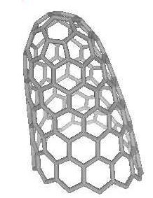
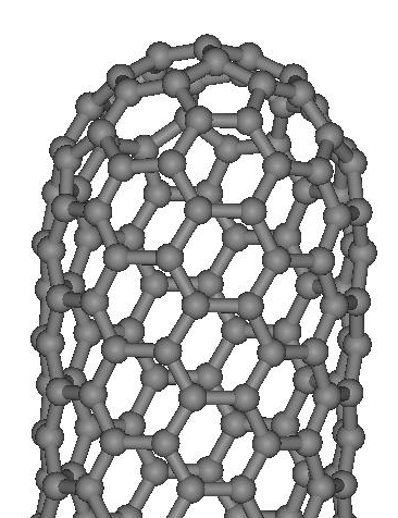
The nanotubes, discovered by Ijima
(see [3] and Figs. 6,7), are for
now the most studied carbon nanostructures. The nanotubes are
the tubes made from graphene plain, with one (Single Walled)
or more than one (Multiwalled) layers. Sometimes they could
have the cap at their ends (see Fig.6).
The carbon nanotubes (CNTs) are
produced using four main methods: arc discharge of graphite
electrodes in inert atmospheres [3],
pyrolysis of hydrocarbons over catalysts [21],
laser vaporization of graphite targets [22],
and electrolysis of graphite electrodes in the molten salts
[23]. Generally speaking, the
number of techniques used to produce CNTs is growing day by
day, and according to the recent data [24],
even the methane burning in our kitchen produces some quantity
of nanotubes and other carbon nanocrystalls! This fact raises
an important question about the nano-pollution of the environment
and the influence of the nanostructures over our health, and
this is the question still to be solved.
|
|
Figure
6. The capped carbon nanotube
|
|
|
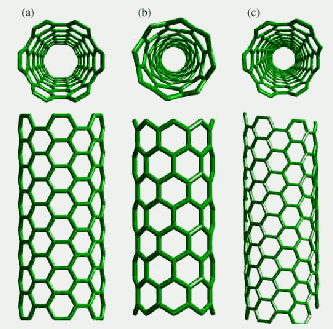
The main parameters determining
their type are their diameter and chirality. The chirality,
or the orientation of six-folds in the nanotube, is an internal
property, but it determines their stability (their quantity
in the experiment) and electronic properties (theoretically
shown by Hamada in [25]). The
plain graphene, being a semiconducting material, in the form
of the nanotubes could have the dielectric, and even the metallic
properties. This fact determines the usage of the metallic CNTs
as field emitters, even their commercial application in the
flat panel displays (the prototype of flat panel display for
TV on the carbon nanotubes was presented by Samsung in 1999),
and as emitters in the electronic microscopy. It is interesting
to note that recently the similar silicon nanotubes were produced
[26], and they have the common
dependence between chirality and metallization. One can speculate,
that this fact could be applied also for other two-dimensional
systems; but unfortunately the other materials suitable for
nanotubes, like boron nitride and molybdenum disulfide, are
dielectric.
|
|
Figure
7. Some types of nanotubes: (a) armchair, (b) zigzag, and (c)
chiral tubes. From the review [15]
|
Another interesting property of carbon nanotubes is
their strength. Indirect measurements [27]
revealed that multi-walled carbon nanotubes possess a Youngs modulus
around 1.8 TPa, i. e. 100 times larger than steel! The robustness
of the nanotubes, in combination with their low weight, leads to the
rising of some fantastic technical projects, such as a space lift.
However, the challenge of building a super-strong composite material
out of nanotubes is still underway.
There are also many other possible applications of the
carbon nanotubes - for example, the quantum wires, chemical sensors
(because of their high specific surface, the electrical resistance
of the tubes is distinctly changing in the presence of some chemical
compounds), and so on. The future developments in the nanotechnology
promise the revolution in all the scopes of humans activity; although
this revolution could be only a myth, the carbon nanotubes are for
now the major breakthrough in the technological development.
Negatively
curved nanostructures
|
|
|
|
|
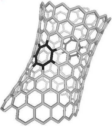
Figure
8. The nanotube with two sevenfolds (black)
|
Figure
10. The high genus fullerene. From the review [10]
|
|
As it was mentioned earlier, the
inclusion of the heptagons in the hexagonal lattice leads to
the appearance of negative curvature.
|
|
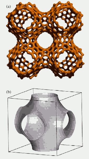
Figure
9. The four cells of Schwarzite (a) and the TPMS (b). From the
review [10]
|
The single sevenfold in the plain graphene lattice
was theoretically studied in [14],
but this situation, unfortunately, has not been observed in the experiment
yet. The heptagons were observed in the nanotubes ([28],
Fig. 8), and in the work [29] the magnetic
properties of negatively curved structures were calculated. The heptagon
included into the graphene layer bends it into a buckled surface;
and symmetrical adding of the heptagons into the nanotube leads to
the geometry of one-sheet hyperboloid, as it is shown in Fig.8.
Another type of negatively curved periodical nanostructures
was proposed by Terrones [10]; he supposed
that a mathematical object called Triple Periodical Minimal Surface
(TPMS) could be found in the nature, in the form of carbon zeolite-like
structures; he called them Schwarzites (Fig.9). They appear to be
some kind of cubic lattice, but they are two-dimensional structures
and thus their properties differ from those we have in the ordinary
crystalline materials. The energetic calculations performed for Schwarzites
in the work [30], shows, that they
are more stable than C60. Some possible applications of Schwarzites,
according to Terrones [10], are semiconducting
nanodevices, new catalysts and molecular sieves. So, the presence
of the heptagons in the lattice could lead to the increase of stability
for such structure. Thats why Terrones proposed also the existence
of such exotic structures, like high genus fullerenes (Fig. 10).
Although this strange structure has a quasi-spherical shape, it contains
only hexagons and heptagons, and therefore its curvature is negative.
It is topologically similar to the sphere with twenty-one handles.
An important feature of the complex graphitic structures is that they
exhibit holes of labyrinths, in which molecules can be inserted. The
calculations showed that around the holes (necks), the electronic
behavior is metallic [31].
Among other types of exotic structures, containing
heptagons as well as pentagons with hexagons, one can mention the
toroidal structure [7], helicoidal graphitic
tube [8] and the Haeckelites [10].
The Haeckelites, named in honor of German zoologist Ernst Haeckel,
are the structures with variable shape geometries, including planar;
they consist of fivefolds and hexagons with the required number of
sevenfolds added to negate the curvature. One should note, that according
to [10] the Haeckelites are metallic
(they have non-zero density of states on the Fermi energy).
Electronic
structure of various carbon nanoparticles
|
|
There are many different methods
to calculate the electronic structure of the carbon lattice,
including the tight-binding and ab initio calculations,
the k· p approximation, and the evolution
of this approach, giving the two-dimensional Dirac equation
(one can call it a sublattice approximation, since two components
of the Dirac equation appeared on the two sublattices). As it
was shown above, the main feature of the nanostructures is their
geometrical properties. As usual, the ab initio and tight-binding
methods operate with nanostructure as with three-dimensional
objects. The k· p and sublattice
approximations, like a band model for the carbon nanotubes [32],
work with the 2D - shape of the structure.
|
|
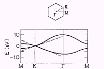
Figure
11. The band structure of the planar graphite (π -orbitals)
[34]
|
As for the single-electron approximation, one can introduce
the local density of states (LDoS) as the main parameter describing
the electronic properties of the system. The theory for band structure
of graphite was developed in 1947 by Wallace [33].
As it is shown in Fig. 11, near the corner K of the Brillouin zone
of the planar graphite (and near all the other corners) the dispersion
law could be approximated with the linear function, as in the massless
Dirac (or Weyl) equation; and this leads to the sublattice approximation
mentioned above. One should also notice, that at the Fermi energy
there are two independent wave functions, located on the two sublattices
[34].
In the presence of the five and / or sevenfolds, one
needs to take into account two independent things: a boundary condition
for the Dirac spinor function, and a topologically non trivial gauge
field. The first factor was mentioned in the works [35,36].
In these articles, an elegant approach to the defect systems was proposed,
and the boundary conditions for the initial Schrödinger equation lead
to the nontrivial boundary conditions for the spinors, and finally
to the fields of the defect. Nevertheless, the second factor was not
taken into consideration. This factor was known mostly in the elasticity
theory [37]; in the field of electronic
structure of nanoparticles, it was introduced in the work [38],
and in the recent work [39] it was
used to describe the electronic structure of the carbon nanohorns
(see Fig.4 in the Chapter 2). The spinor boundary conditions in these
articles were not taken into account as in [35,36],
and for this reason the proposed model was criticized [40].
An attempt of full description of the system was made in [41];
however, this is still a subject for the discussion.
|
|
In contrast to the defect structures, the electronic
states of the nanotubes is a well investigated topic, in both
theoretical and experimental aspects. The translational and
rotational symmetries of the nanotube, being similar to the
symmetries of the solids, result in the band theory [25].
The essence of this theory could be formulated in a very compact
and simple form. Actually, lets plot a Brillouin zone and the
lines of constant wave vector in the momentum space (Fig. 12).
The orientation of the Brillouin zone depends on the type of
the tube (armchair, zigzag etc.), and the distance between
the lines (its dimension is converse length) depends on the
radius of the tube; if the line is crossing the hexagons corner,
the phase of the wavefunction could take an exact zero value,
and this result in the metallization of the (sub)lattice. The
similar condition for the zero phase was used to describe a
metallization of the carbon nanocones in [36].
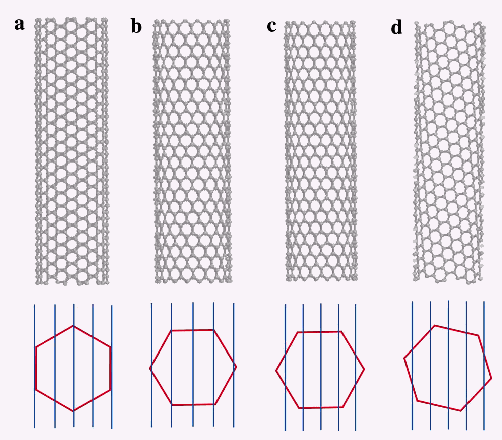
An example of the metallic behavior is shown in Fig.12 (a).
On the contrary, in Fig. 12 (c,d) this condition is not satisfied,
and these tubes are semiconducting. This results in the, respectively,
zero or non-zero electronic density of states on the Fermi level.
When the lines are close to the hexagon corners, as it is shown
in Fig. 12(b), the width of the band-gap is small. The connection
of the metallic and semiconducting tube of the type (a) and
(b) could lead to the nanoscale semiconducting device like a
diode or field transistor (FET).
|
|
Figure
12. (a) Armchair, (b,c) zig-zag and (d) chiral tube; (a) metallic,
(b) small gap semiconductor, and (c,d) semiconductor. From the
review [42]
|
The
realization of the connection, proposed by many different authors
[43], may be a chirality-changing pentagon
- heptagon pair included into a nanotube structure. The practical
use of such devices is expected in the very near future.
Conclusion
At the end of this review, one needs to remember the
words of Richard Feynman: ... there is plenty of room at the bottom.
This statement was made in 1959, and its meaning reflects the (possible)
significance of the molecular scale devices. In his lecture at the
California Institute of Technology, Feynman proposed the new ideas
to be realized on the molecular size level the information on the
nanoscale, miniaturized and quantum computers, and the extensively
advertised concept of nano - bots. And what do we see at the present
time? On the one hand, there is a popularized idea of nano robots,
which will appear to build any thing in no time and without any cost;
but there are no ideas (even in the theoretical aspect) how these
systems should look like. There are many enthusiasts of this approach
[44], but they lack the practical techniques
which are needed to convert their dreams into the scientific and technical
reality. On the other hand, there are some types of the nanostructures
(the quantum dots, semiconducting heterostructures and the carbon
nanostructures described above) which are investigated enough, and
some of them have commercial applications (see Chapter 4). The most
important thing we need to do now is to develop the present technologies
in accordance with the present state of the science and with the requirements
of the mankind. The highly advertised nanorobots would be just a little
part of the wonders of future engineering. Both the development and
use of the novel technologies are in our hands; our duty is to manage
them in the worthy way.
References
- IEEE Trans. Plasma
Sci. 32, 2152 (2004)
- Kroto H. W. et al.,
Nature 318 162 (1985)
- Ijima S. Nature (London)
354 56 (1991)
- Dorset D. L., Fryer
J. R., J. Phys. Chem. B 105 2356 (2001)
- Kuzuo R. et al., Phys.
Rev. B 49 5054 (1994)
- Ge M. And Sattler
K., Chem. Phys. Lett. 220 192 (1994)
- Itoh S. et al., Phys.
Rev B 47 1703 (1993)
- Amelinckx S. et al.,
Science 265 635 (1994)
- Mackay A. L. and Terrones
H., Nature 352 762 (1991)
- H.Terrones and M.Terrones,
New Journal of Physics 5 126 (2003)
- Chopra N. G. et.
al., Science 269 966 (1995)
- Tenne R. et al.,
Nature 360 444 (1992)
- Rurali R. and Lorente
N., Phys.Rev.Lett. 94 026805 (2005)
- Nelson D. R. and
Peliti L., J. Phys. (Paris) 48, 1085 (1987)
- Terrones H. and Terrones
M., New Jorn. Phys. 5 126.1 (2003)
- Krishnan A. et al.,
Nature 388 451 (1997)
- Ijima S. et al.,
Chem Phys. Lett. 309 165 (1999)]
- Taikawa H. et al.,
Physica B 323 277 (2002)
- Bonard J.-M. et al.,
Jorn. Appl. Phys. 91 10107 (2002)
- Fleming R. M. et
al., Nature 352 787 (1991)
- Terrones M. et al.,
Nature 388 52 (1997)
- Tress A. et al.,
Science 273 483 (1996)
- Hsu W. K. et al.,
Nature 377 687 (1995)
- J. Mater. Sci. 39
2199 (2004)
- Hamada N. et al.,
Phys. Rev. Lett. 68 1579 (1992)
- Phys.Rev.Lett. 94
026805 (2005)
- Treacy M. M. et al.,
Nature 381 678 (1996)
- Weldon D. N. et al.,
Chem. Phys. Lett. 241 365 (1995)
- Park N. et al., Phys.
Rev. Lett. 91 237204-2 (2003)
- Lenosky T. et al.,
Nature 355 333 (1992)
- Ricardo-Chavez J.
L. et al., Phys. Rev. B 56 12143 (1997)
- Saito R. et al.,
Phys. Rev. B 46 1804 (1992)
- Wallace P. R., Phys.
Rev. 71 622 (1947)
- DiVincenzo D. P.
and Mele E. J., Phys. rev.B 29 1685 (1984)
- Lammert P. and Crespi
V. H., Phys.Rev.Lett. 85 5190 (2000)
- Lammert P. and Crespi
V. H., Phys.Rev.B 69 035406 (2004)
- Landau L. and Lifshitz
E. M., Theory of elasticity, Pergamon, London (1965)
- Osipov V. A. et al.,
JETP 96 140 (2003)
- Kolesnikov D. V.
and Osipov V. A., JETP Lett., 79 660 (2004)
- Compernolle S. et
al., Journ. Chem. Phys. 121 2326 (2004)
- Osipov V.A. and Kolesnikov
D.V., Romanian Journal of Physics, to be published (2005)
- Dai H., Sur.Sci.
500 218 (2002)
- Chiko L. et al.,
Phys. Rev. Lett. 76 991 (1996)
- Drexler Erik K.,
Engines of Creation, Anchor Books (1986); avaliable online
on the www.foresight.org/EOC/
|